You've followed the rumors and twitter home sex videosignored the hype; you waited for the reviews and looked at all the benchmarks. Finally, you slapped down your dollars and walked away with one of the latest graphics cards from AMD or Nvidia. Inside these, lies a large graphics processor, packed with billions of transistors, all running at clock speeds unthinkable a decade ago.
You're really happy with your purchase and games never looked nor played better. But you might just be wondering what exactly is powering your brand new Radeon RX 5700 and how different is it to the chip in a GeForce RTX.
Welcome to our architectural and feature comparison of the newest GPUs from AMD and Nvidia: Navi vs Turing.
Anatomy of a Modern GPU
Before we begin our breakdown of the overall chip structures and systems, let's take a look at the basic format that all modern GPUs follow. For the most part, these processors are just floating point (FP) calculators; in other words, they do math operations on decimal/fractional values. So at the very least, a GPU needs to have one logic unit dedicated to these tasks and they're usually called FP ALUs(floating point arithmetic logic units) or FPUs for short. Not all of the calculations that GPUs do are on FP data values, so there will also be an ALU for whole number (integer) math operations or it might even be the same unit, that just handles both data types.
Now, these logic units are going to need something to organize them, by decoding and issuing instructions to keep them busy, and this will be in the form of at least one dedicated group of logic units. Unlike the ALUs, they won't be programmable by the end user; instead, the hardware vendor will ensure this process is managed entirely by the GPU and its drivers.
To store these instructions and the data that needs to be processed, there needs to be some kind of memory structure, too. At its simplest level, it will be in two forms: cacheand a spot of local memory. The former will be embedded into the GPU itself and will be SRAM. This kind of memory is fast but takes up a relative large amount of the processor's layout. The local memory will be DRAM, which is quite a bit slower than SRAM and won't normally be put into the GPU itself. Most of the graphics cards we see today have local memory in the form of GDDRDRAM modules.
Finally, 3D graphics rendering involves additional set tasks, such as forming triangles from vertices, rasterizing a 3D frame, sampling and blending textures, and so on. Like the instruction and control units, these are fixed functionin nature. What they do and how they operate is completely transparent to users programming and using the GPU.
Let's put this together and make a GPU:
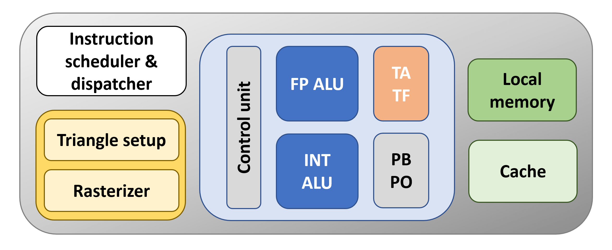
The orange block is the unit that handles textures using what are called texture mapping units(TMUs) - TA is the texture addressingunit – it creates the memory locations for the cache and local memory to use – and TF is the texture fetch unit that collects texture values from memory and blends them together. These days, TMUs are pretty much the same across all vendors, in that they can address, sample and blend multiple texture values per GPU clock cycle.
The block beneath it writes the color values for the pixels in the frame, as well as sampling them back (PO) and blending them (PB); this block also performs operations that are used when anti-aliasing is employed. The name for this block is render output unitor render backend(ROP/RB for short). Like the TMU, they're quite standardized now, with each one comfortably handling several pixels per clock cycle.
Our basic GPU would be awful, though, even by standards from 13 years ago. Why?
There's only one FPU, TMU, and ROP. Graphics processors in 2006, such as Nvidia's GeForce 8800 GTX had 128, 32, and 24 of them, respectively. So let's start to do something about that....
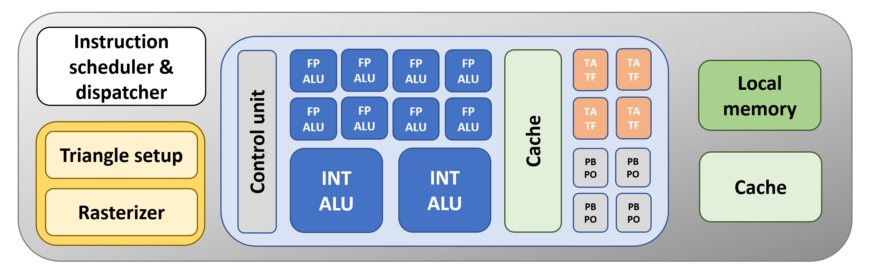
Like any good processor manufacturer, we've updated our GPU by adding in some more units. This means the chip will be able to process more instructions simultaneously. To help with this, we've also added in a bit more cache, but this time, right next to the logic units. The closer cache is to a calculator structure, the quicker it can get started on the operations given to it.
The problem with our new design is that there's still only one control unit handling our extra ALUs. It would be better if we had more blocks of units, all managed by their own separate controller, as this would mean we could have vastly different operations taking place at the same time.
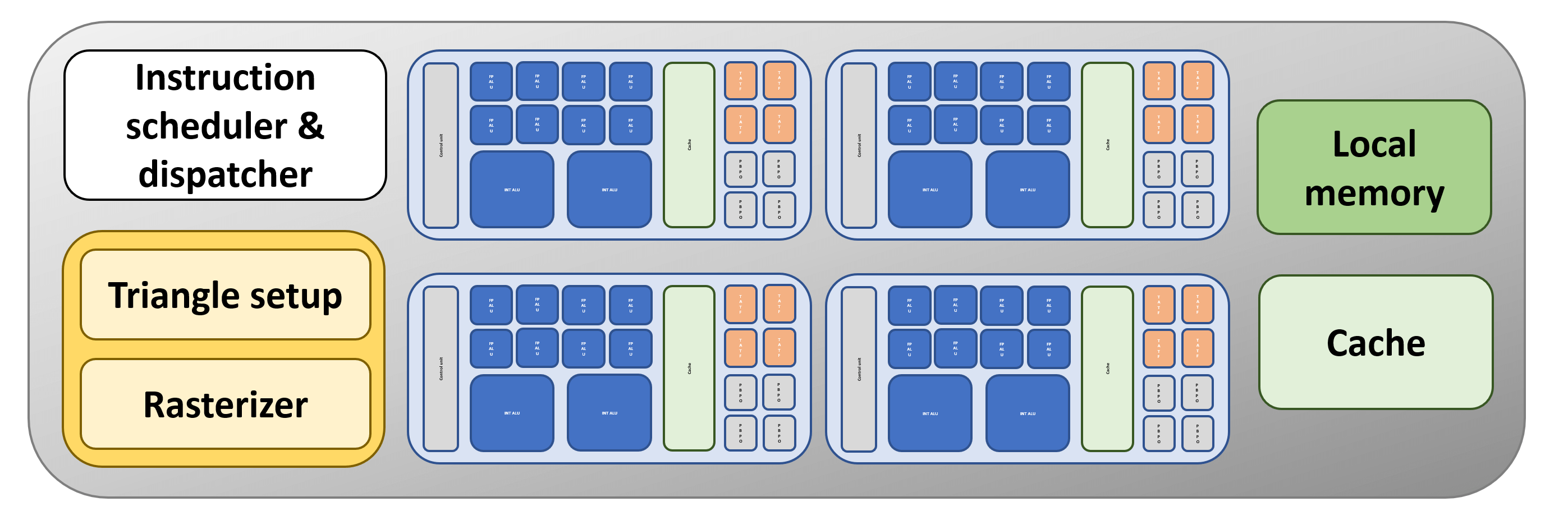
Now this is more like it! Separate ALU blocks, packed with their own TMUs and ROPs, and supported by dedicated slices of tasty, fast cache. There's still only one of everything else, but the basic structure isn't a million miles away from the graphics processor we see in PCs and consoles today.
Navi and Turing: Godzilla GPUs
Now that we have described the basic layout of a graphics chip, let's start our Navi vs. Turing comparison with some images of the actual chips, albeit somewhat magnified and processed to highlight the various structures.
On the left is AMD's newest processor. The overall chip design is called Navi (some folks call it Navi 10) and the graphics architecture is called RDNA. Next to it, on the right, is Nvidia's full size TU102 processor, sporting the latest Turing architecture. It's important to note that these images are not to scale: the Navi die has an area of 251 mm2, whereas the TU102 is 752 mm2. The Nvidia processor is big, but it's not 8 times bigger than the AMD offering!
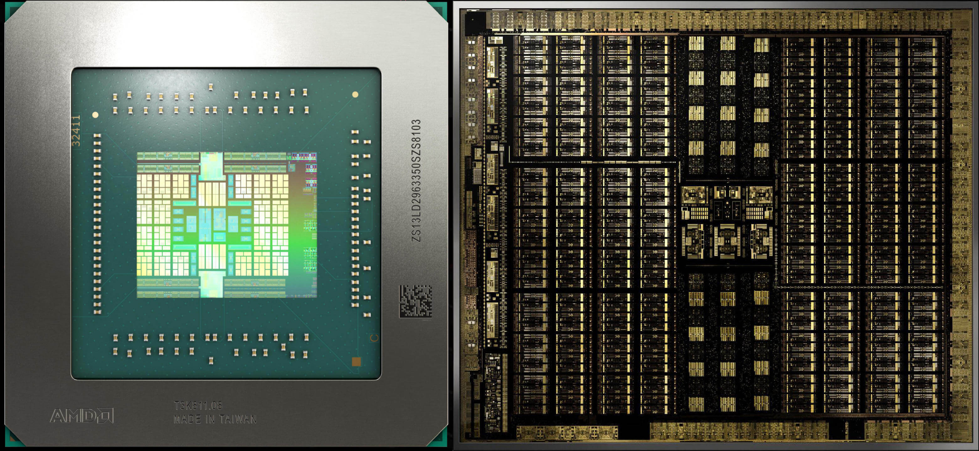
They're both packing a gargantuan number of transistors (10.3 vs 18.6 billion) but the TU102 has an average of ~25 million transistors per square mm compared to Navi's 41 million per square mm.
This is because while both chips are fabricated by TSMC, they're manufactured on different process nodes: Nvidia's Turing is on the mature 12 nm manufacturing line, whereas AMD's Navi gets manufactured on the newer 7 nm node.
Just looking at images of the dies doesn't tell us much about the architectures, so let's take a look at the GPU block diagrams produced by both companies.
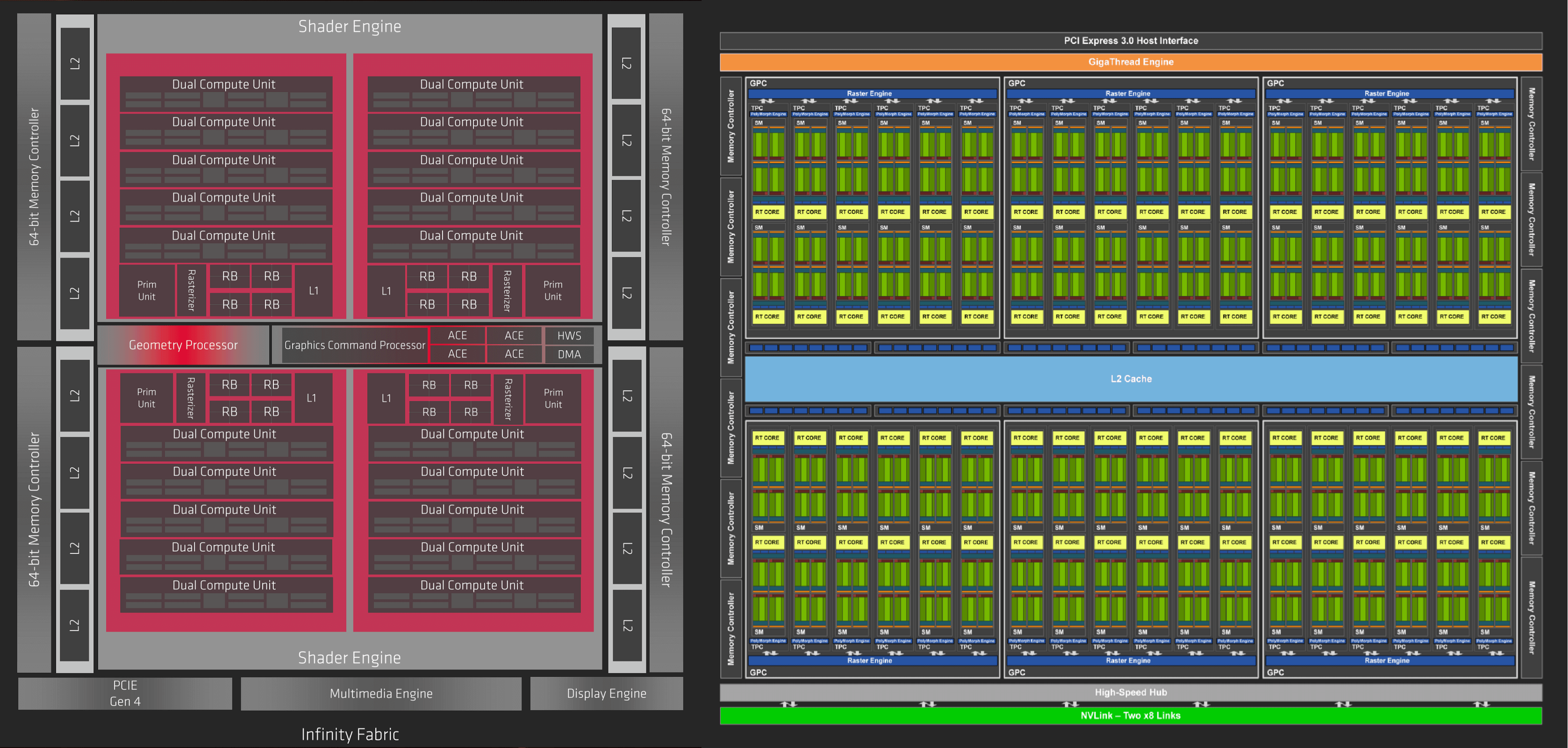
The diagrams aren't meant to be a 100% realistic representation of the actual layouts but if you rotate them through 90 degrees, the various blocks and central strip that are apparent in both can be identified. To start with, we can see that the two GPUs have an overall structure like ours (albeit with more of everything!).
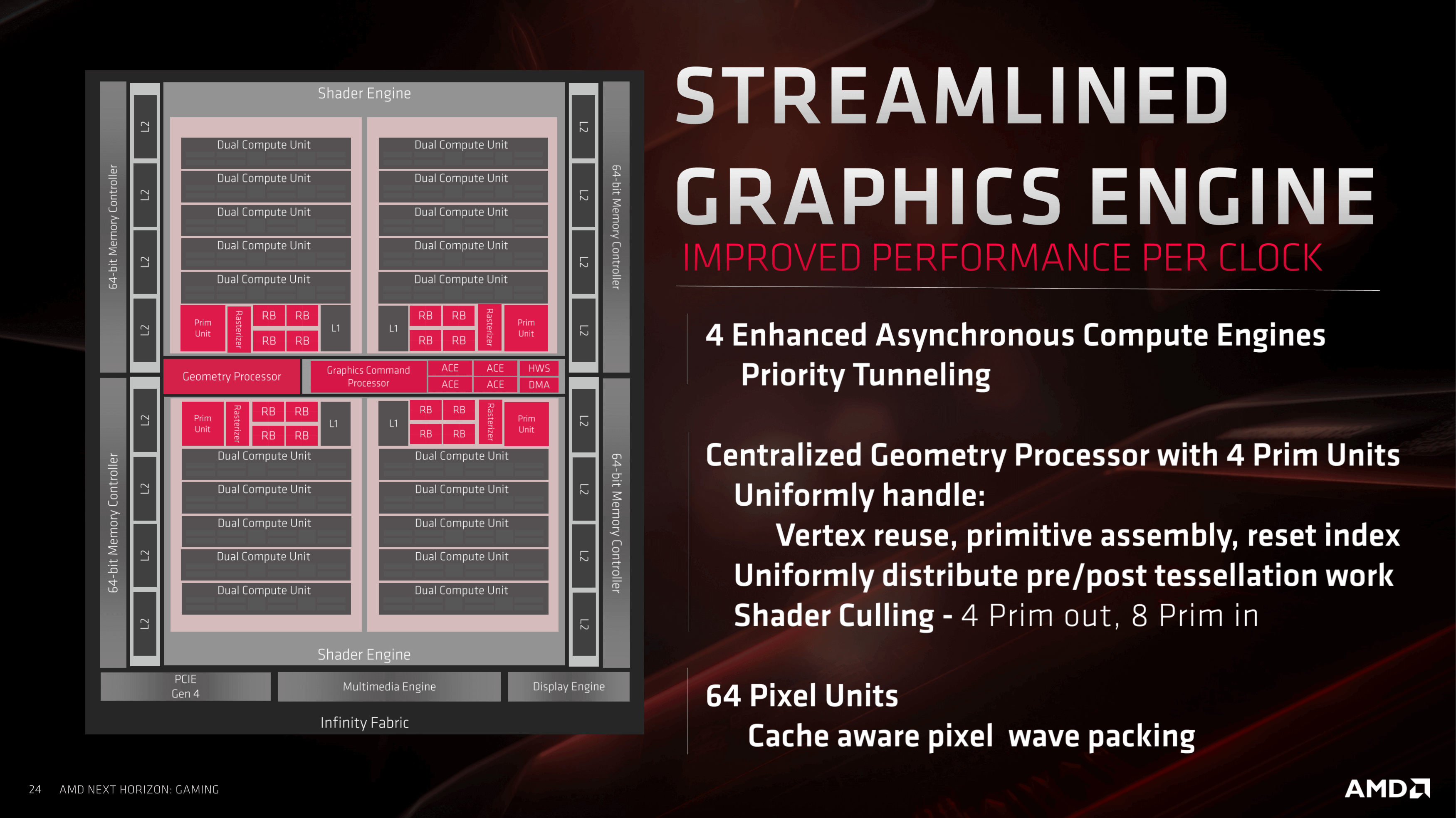
Both designs follow a tiered approach to how everything is organised and grouped – taking Navi to begin with, the GPU is built from 2 blocks that AMD calls Shader Engines (SEs), that are each split into another 2 blocks called Asynchronous Compute Engines(ACEs). Each one of these comprises 5 blocks, titled Workgroup Processors (WGPs), which in turn consist of 2 Compute Units(CUs).
For the Turing design, the names and numbers are different, but the hierarchy is very similar: 6 Graphics Processing Clusters(GPCs), each with 6 Texture Processing Clusters(TPCs), with each of those built up of 2 Streaming Multiprocessor(SM) blocks.
If you picture a graphics processor as being a large factory, where different sections manufacture different products, using the same raw materials, then this organization starts to make sense. The factory's CEO sends out all of the operational details to the business, where it then gets split into various tasks and workloads. By having multiple, independentsections to the factory, the efficiency of the workforce is improved. For GPUs, it's no different and the magic keyword here is scheduling.
Front and Center, Soldier – Scheduling and Dispatch
When we took a look at how 3D game rendering works, we saw that a graphics processor is really nothing more than a super fast calculator, performing a range of math operations on millions of pieces of data. Navi and Turing are classed as Single Instruction Multiple Data(SIMD) processors, although a better description would be Single Instruction Multiple Threads (SIMT).
A modern 3D game generates hundreds of the threads, sometimes thousands, as the number of vertices and pixels to be processed is enormous. To ensure that they all get done in just a few microseconds, it's important to have as many logic units as busy as possible, without the whole thing stalling because the necessary data isn't in the right place or there's not enough resource space to work in.
When we took a look at how 3D game rendering works, we saw that a graphics processor is really nothing more than a super fast calculator, performing a range of math operations on millions of pieces of data. Navi and Turing are classed as Single Instruction Multiple Data (SIMD) processors, although a better description would be Single Instruction Multiple Threads (SIMT).
Navi and Turing work in a similar manner whereby a central unit takes in all the threads and then starts to schedule and issue them. In the AMD chip, this role is carried out by the Graphics Command Processor; in Nvidia's, it's the GigaThread Engine. Threads are organized in such a way that those with the same instructions are grouped together, specifically into a collection of 32 threads.
AMD calls this collection a wave, whereas Nvidia call it a warp. For Navi, one Compute Unit can handle 2 waves (or one 64 thread wave, but this takes twice as long), and in Turing, one Streaming Multiprocessor works through 4 warps. In both designs, the wave/warps are independent, i.e. they don't need the others to finish before they can start.
So far then, there's not a whole lot different between Navi and Turing – they're both designed to handle a vast number of threads, for rendering and compute workloads. We need to look at what processes those threads to see where the two GPU giants separate in design.
A Difference of Execution - RDNA vs CUDA
AMD and Nvidia take a markedly different approach to their unified shader units, even though a lot of the terminology used seems to be the same. Nvidia's execution units (CUDA cores) are scalarin nature – that means one unit carries out one math operation on one data component; by contrast, AMD's units (Stream Processors) work on vectors– one operation on multiple data components. For scalar operations, they have a single dedicated unit.
Before we take a closer look at the execution units, let's examine AMD's changes to theirs. For 7 years, Radeon graphics cards have followed an architecture called Graphics Core Next (GCN). Each new chip has revised various aspects of the design, but they've all fundamentally been the same.
AMD has provided a (very) brief history of their GPU architecture:
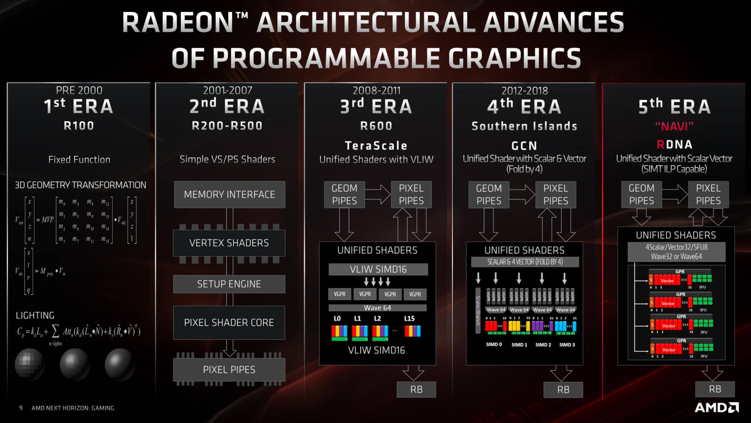
GCN was an evolution of TeraScale, a design that allowed for large waves to processed at the same time. The main issue with TeraScale was that it just wasn't very friendly towards programmers and needed very specific routines to get the best out of it. GCN fixed this and provided a far more accessible platform.
The CUs in Navi have been significantly revised from GCN as part of AMD's improvement process. Each CU contains two sets of:
- 32 SPs (IEE754 FP32 and INT32 vector ALUs)
- 1 SFU
- 1 INT32 scalar ALU
- 1 scheduling and dispatch unit
Along with these, every CU contains 4 texture units. There are other units inside, to handle the data read/writes from cache, but they're not shown in the image below:
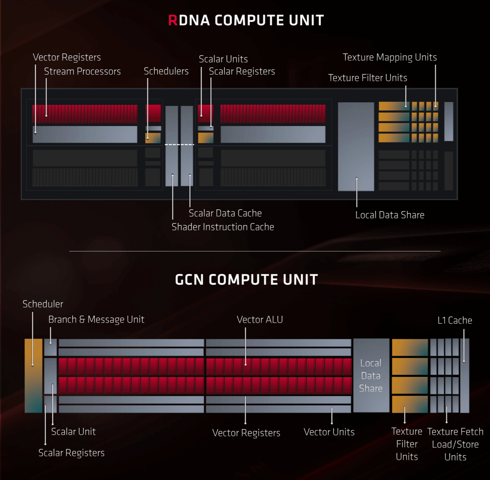
Compared to GCN, the setup of an RDNA CU might seem to be not very different, but it's how everything has been organized and arranged that's important here. To start with, each set of 32 SPs has its own dedicated instruction unit, whereas GCN only had one schedule for 4 sets of 16 SPs.
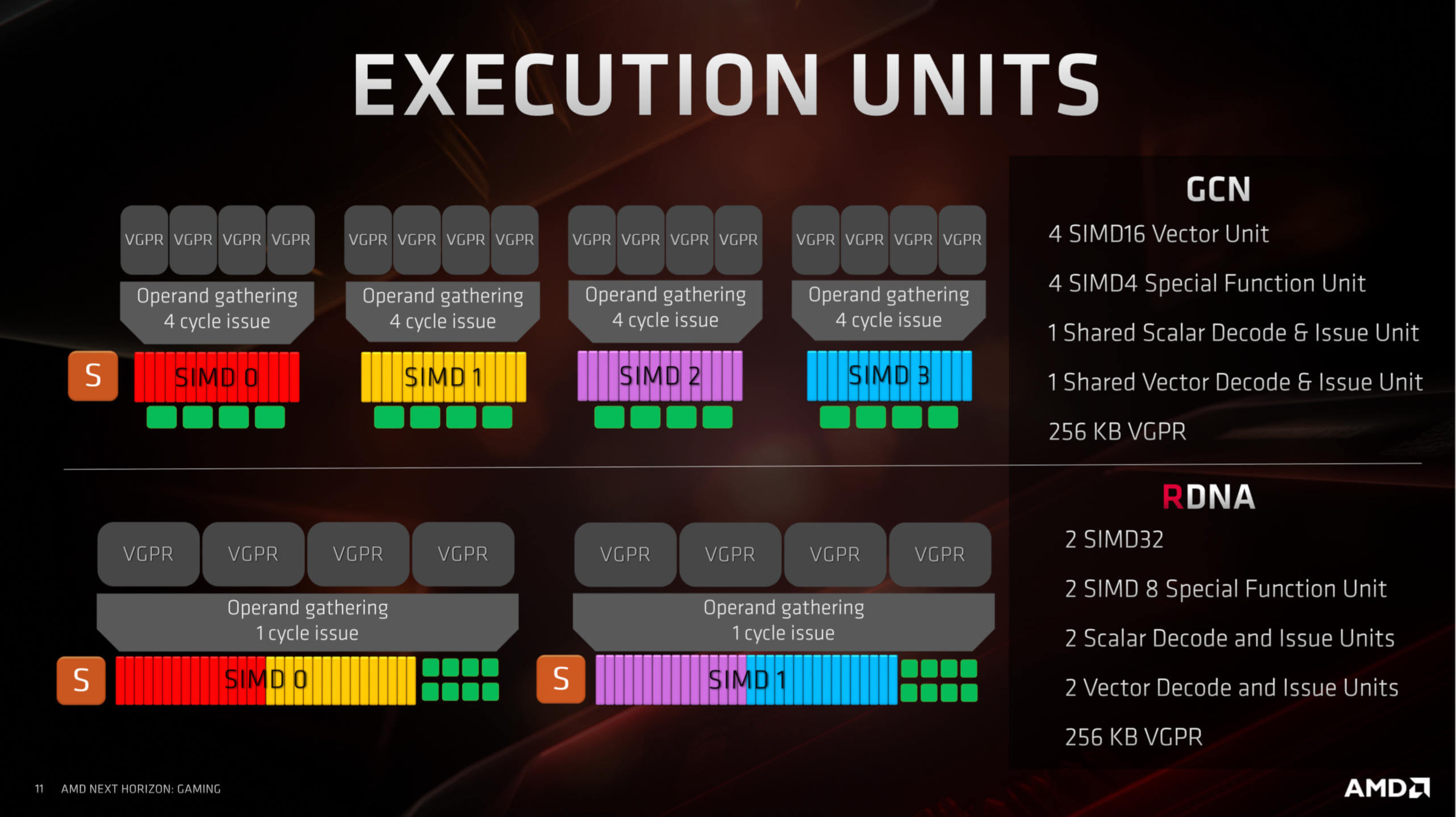
This is an important change as it means one 32 thread wave can be issued per clock cycle to each set of SPs. The RDNA architecture also allows the vector units to handle waves of 16 threads at twice the rate, and waves of 64 threads at half the rate, so code written for all of the previous Radeon graphics cards is still supported.
For game developers, these changes are going to be very popular.
For scalar operations, there are now twice as many units to handle these; the only reduction in the number of components is in the form of the SFUs – these are special functionunits, that perform very specific math operations, e.g. trigonometric (sine, tangent), reciprocal (1 divided by a number) and square roots. There's less of them in RDNA compared to GCN but they can now operate on data sets twice the size as before.
For game developers, these changes are going to be very popular. Older Radeon graphics cards had lots of potential performance, but tapping into that was notoriously difficult. Now, AMD has taken a large step forward in reducing the latency in processing instructions and also retained features to allow for backwards compatibility for all the programs designed for the GCN architecture.
But what about for the professional graphics or compute market? Are these changes beneficial to them, too?
The short answer would be, yes (probably). While the current version of the Navi chip as found in the likes of the Radeon RX 5700 XT, has fewer Stream Processors that the previous Vega design, we found it to outperform a previous-gen Radeon RX Vega 56 quite easily:
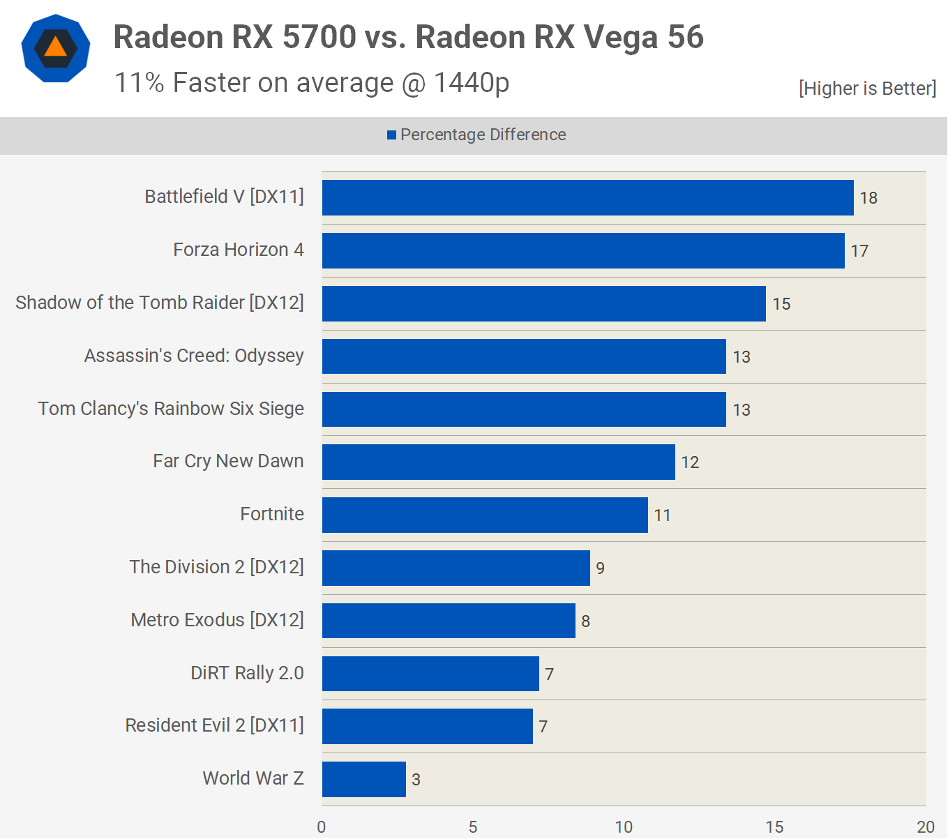
Some of this performance gain will come from the RX 5700 XT higher clock rate than the RX Vega 56 (so it can write more pixels per second into the local memory) but it's down on peak integer and floating point performance by as much as 15%; and yet, we saw the Navi chip outperform the Vega by as much as 18%.
Professional rendering programs and scientists running complex algorithms aren't exactly going to be blasting through a few rounds of Battlefield V in their jobs (well, maybe...) but if the scalar, vector, and matrix operations done in a game engine are being processed faster, then this shouldtranslate into the compute market. Right now, we don't know what AMD's plans are regarding the professional market – they could well continue with the Vega architecture and keep refining the design, to aid manufacturing, but given the improvements in Navi, it makes sense for the company to move everything onto the new architecture.
Nvidia's GPU design has undergone a similar path of evolution since 2006 when they launched the GeForce 8 series, albeit with fewer radical changes than AMD. This GPU sported the Tesla architecture, one of the first to use a unified shader approach to the execution architecture. Below we can see the changes to the SM blocks from the successor to Tesla (Fermi), all the way through to Turing's predecessor (Volta):
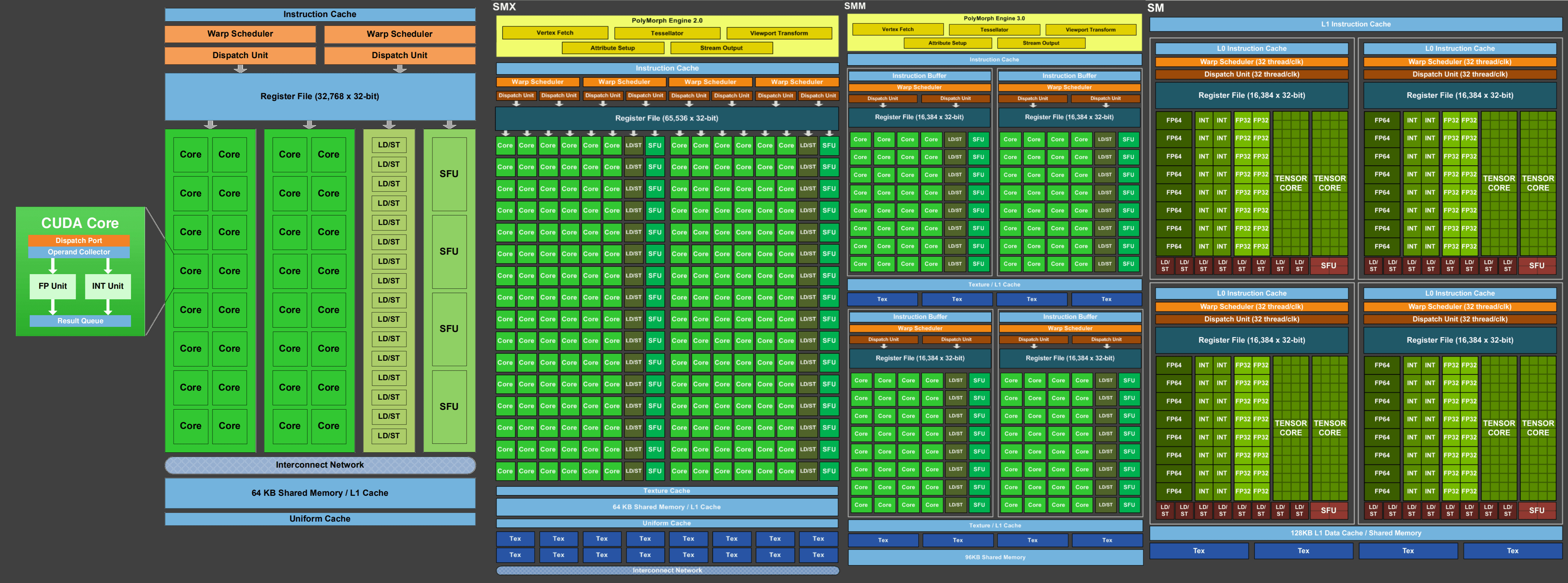
As mentioned earlier in this article, CUDA cores are scalar. They can carry out one float and one integer instruction per clock cycle on one data component (note, though, that the instruction itself might take multiple clock cycles to be processed), but the scheduling units organize them into groups in such a way that, to a programmer, they can perform vector operations. The most significant change over the years, other than there simply being more units, involves how they are arranged and sectioned.
In the Kepler design, the full chip had 5 GPCs, with each one housing three SM blocks; by the time Pascal appeared, the GPCs were split into discrete sections (TPCs) with two SMs per TPC. Just like with the Navi design. this fragmentation is important, as it allows the overall GPU to be as fully utilized as possible; multiple groups of independent instructions can be processed in parallel, raising the shading and compute performance of the processor.
Let's take a look at the Turing equivalent to the RDNA Compute Unit:
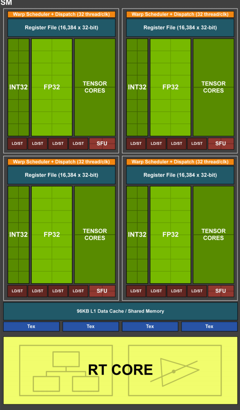
One SM contains 4 processing blocks, with each containing:
- 1 instruction scheduling and dispatch unit
- 16 IEE754 FP32 scalar ALUs
- 16 INT32 scalar ALUs
- 2 Tensor cores
- 4 SFUs
- 4 Load/Store units (which handle cache read/writes)
There are also 2 FP64 units per SM, but Nvidia doesn't show them in their block diagrams anymore, and every SM houses 4 texture units (containing texturing addressing and texturing filtering systems) and 1 RT (Ray Tracing) core.
The FP32 and INT32 ALUs can work concurrently and in parallel. This is an important feature because even though 3D rendering engines require mostly floating point calculations, there is still a reasonable number of simple integer operations (e.g. data address calculations) that need to be done.
The Tensor Cores are specialized ALUs that handle matrix operations. Matrices are 'square' data arrays and Tensor cores work on 4 x 4 matrices. They are designed to handle FP16, INT8 or INT4 data components in such a way that in one clock cycle, up to 64 FMA (fused multiply-then-add) float operations take place. This type of calculation is commonly used in so-called neural networks and inferencing – not exactly very common in 3D games, but heavily used by the likes of Facebook for their social media analyzing algorithms or in cars that have self-driving systems. Navi is also able to do matrix calculations but requires a large number of SPs to do so; in the Turing system, matrix operations can be done while the CUDA cores are doing other math.
The RT Core is another special unit, unique to the Turing architecture, that performs very specific math algorithms that are used for Nvidia's ray tracing system. A full analysis of this is beyond the scope of this article, but the RT Core is essentially two systems that work separately to the rest of the SM, so it can still work on vertex or pixel shaders, while the RT Core is busy doing calculations for ray tracing.
On a fundamental level, Navi and Turing have execution units that offer a reasonably similar feature set (a necessity born out of needing to comply with the requirements of Direct3D, OpenGL, etc.) but...
On a fundamental level, Navi and Turing have execution units that offer a reasonably similar feature set (a necessity born out of needing to comply with the requirements of Direct3D, OpenGL, etc.) but they take a very different approach to how these features are processed. As to which design is better all comes down to how they get used: a program that generates lots of threads performing FP32 vector calculations and little else would seem to favor Navi, whereas a program with a variety of integer, float, scalar and vector calculations would favor the flexibility of Turing, and so on.
The Memory Hierarchy
Modern GPUs are streaming processors, that is to say, they are designed to perform a set of operations on every element in a stream of data. This makes them less flexible than a general purpose CPU and it also requires the memory hierachy of the chip to be optimized for getting data and instructions to the ALUs as quickly as possible and in as many streams as possible. This means that GPUs will have less cache than a CPU as the more of the chip needs to be dedicated to cache access, rather the amount of cache itself.
Both AMD and Nvidia resort to using multiple levels of cache within the chips, so let's have peek at what Navi packs first.

Starting at the lowest level in the hierarchy, the two blocks of Stream Processors utilize a total of 256 kiB of vector general purpose registers (generally called a register file), which is the same amount as in Vega but that was across 4 SP blocks; running out of registers while trying to process a large number of threads really hurts performance, so this is definitely a "good thing." AMD has greatly increased the scalar register file, too. Where it was previously just 4 kiB, it's now 32 kiB per scalar unit.
Two Compute Units then share a 32 kiB instruction L0 cache and a 16 kiB scalar data cache, but each CU gets its own 32 kiB vector L0 cache; connecting all of this memory to the ALUs is a 128 kiB Local Data Share.
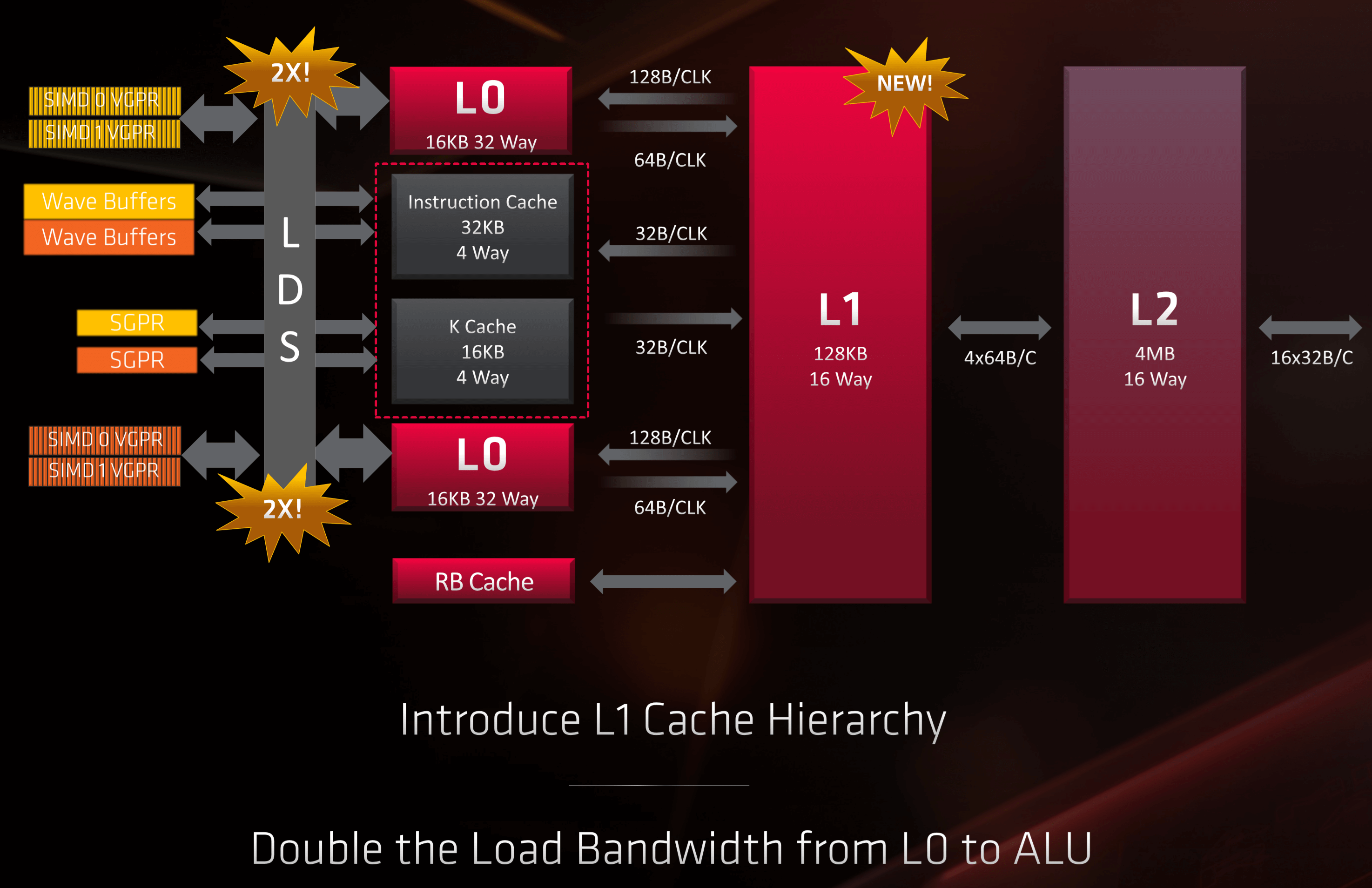
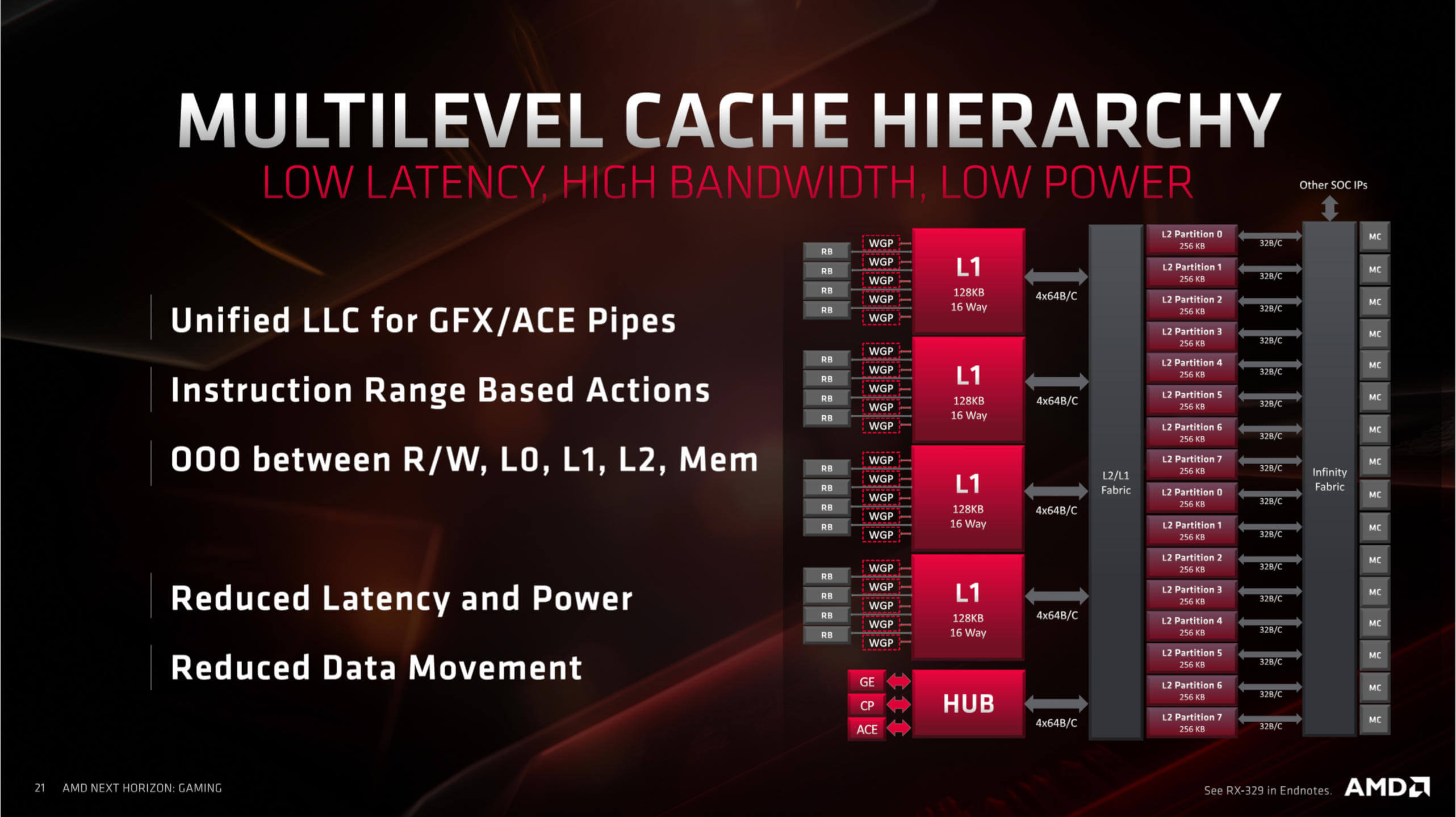
In Navi, two Compute Engines form a Workgroup Processor, and five of those form an Asynchronous Compute Engine (ACE). Each ACE has access to its own 128 kiB of L1 cache and the whole GPU is further supported by 4 MiB of L2 cache, that's interconnected to the L1 caches and other sections of the processor.
This is almost certainly a form of AMD's proprietary Infinity Fabric interconnect architecture as the system is definitely employed to handle the 16 GDDR6 memory controllers. To maximize memory bandwidth, Navi also employs lossless color compression between L1, L2, and the local GDDR6 memory.
Again, all of this is welcome, especially when compared to previous AMD chips which didn't have enough low level cache for the number of shader units they contained. In brief, more cache equals more internal bandwidth, fewer stalled instructions (because they're having to fetch data from memory further away), and so on. And that simply equals better performance.
Onto Turing's hierarchy, it has to be said that Nvidia is on the shy side when it comes to providing in-depth information in this area. Earlier in this article, we saw that each SM was split into 4 processing blocks – each one of those has a 64 kiB register file, which is smaller than found in Navi, but don't forget that Turing's ALUs are scalar, not vector, units.
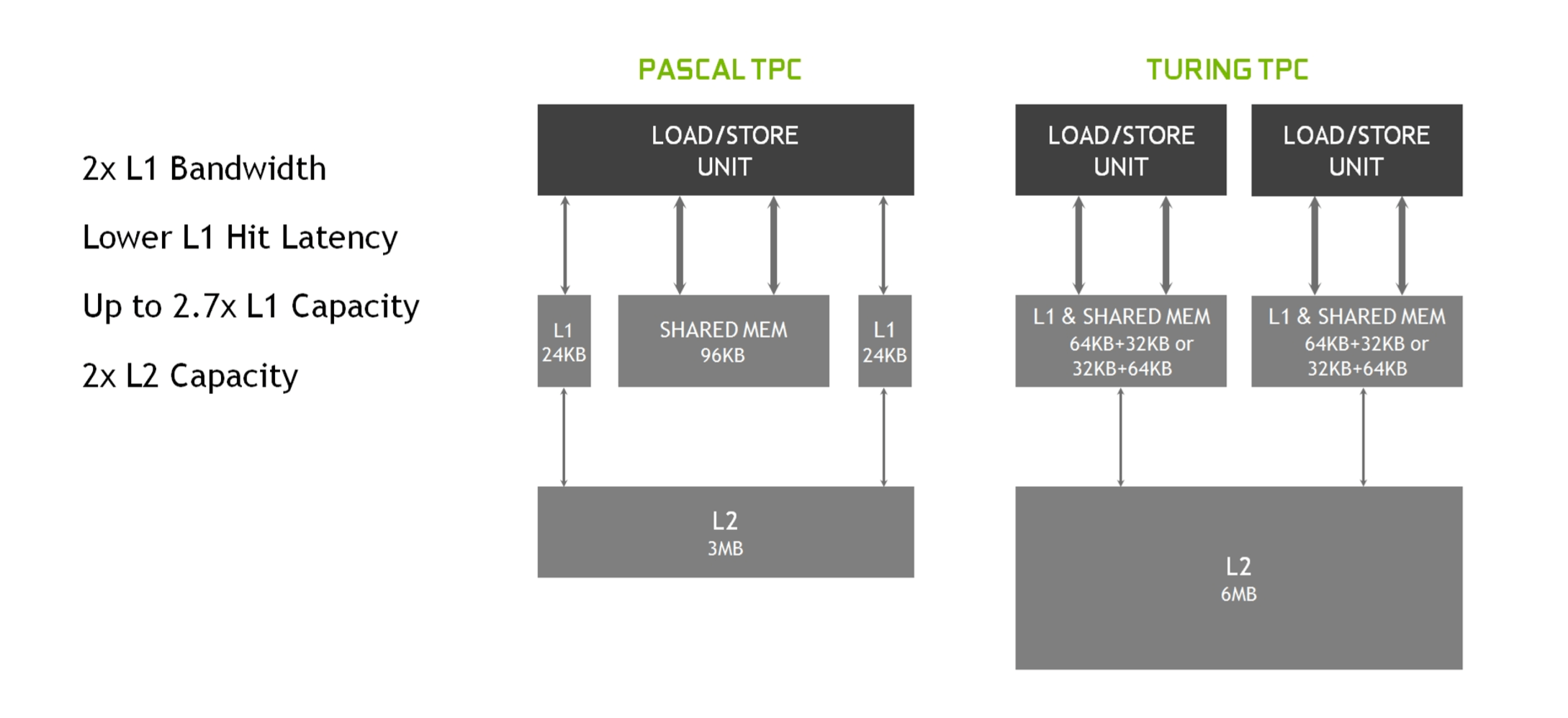
Next up is 96 kiB of shared memory, for each SM, which can be employed as 64 kiB of L1 data cache and 32 kiB of texture cache or extra register space. In 'compute mode', the shared memory can be partitioned differently, such as 32 kiB shared memory and 64 kiB L1 cache, but it's always done as a 64+32 split.
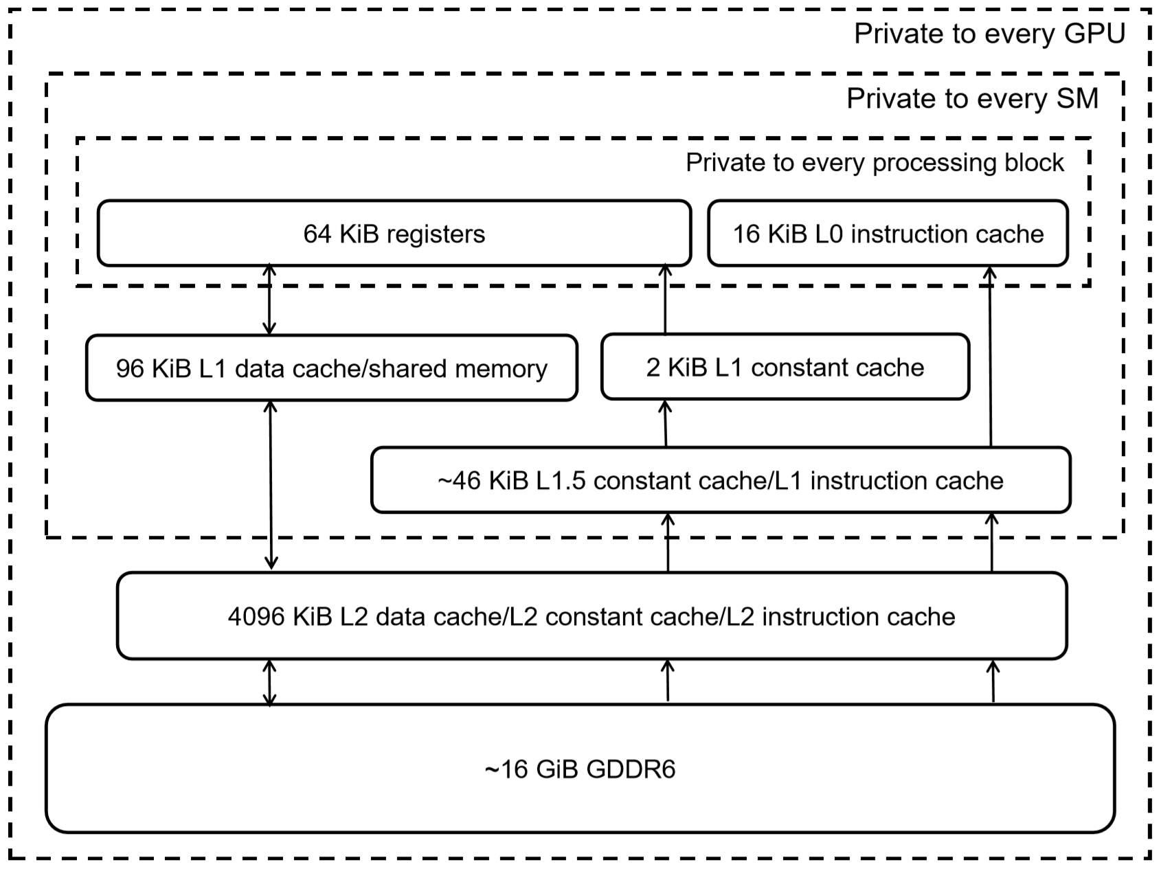
The lack of detail given about the Turning memory system left us wanting more, so we turned to a GPU research team, working at Citadel Enterprise Americas. Of late, they have released two papers, analyzing the finer aspects of the Volta and Turing architectures; the image above is their breakdown of the memory hierarchy in the TU104 chip (the full TU102 sports 6144 kiB of L2 cache).
The team confirmed that the L1 cache throughput is 64 bits per cycle and noted that under testing, the efficiency of Turing's L1 cache is the best of all Nvidia's GPUs. This is on par with Navi, although AMD's chip has a higher read rate to the Local Data Store but a lower rate for the instruction/constant caches.
Both GPUs use GDDR6 for the local memory – this is the most recent version of Graphics DDR SDRAM – and both use 32-bit connections to the memory modules, so a Radeon RX 5700 XT has 8 memory chips, giving a peak bandwidth of 256 GiB/s and 8 GiB of space. A GeForce RTX 2080 Ti with a TU102 chip, runs with 11 such modules for 352 GiB/s of bandwidth and 11 GiB of storage.
AMD's documents can seem to be confusing at times: in the first block diagram we saw of Navi, it shows four 64 bit memory controllers, whereas a later image suggests there are 16 controllers. Given that the likes of Samsung only offer 32 bit GDDR6 memory modules, it would seem that the second image just indicates how many connections there are between the Infinity Fabric system and the memory controllers. There probably are just 4 memory controllers and each one handles two modules.
So overall, there doesn't seem to be an enormous amount of difference between Navi and Turing when it comes to their caches and local memory. Navi has a little more than Turing nearer the execution side of things, with larger instruction/constant and L1 caches, but they're both packed full of the stuff, they both use color compression wherever possible, and both have lots of dedicated GPU die space to maximize memory access and bandwidth.
Triangles, Textures and Pixels
Fifteen years ago, GPU manufacturers made a big deal of how many triangles their chips could process, the number of texture elements that could be filtered each cycle, and the capability of the render output units (ROPs). These aspects are still important today but as 3D rendering technologies require far more compute performance than ever before, the focus is much more on the execution side of things.
However the texture units and ROPs are still worth investigating, if only to note that there is no immediately discernible difference between Navi and Turing in these areas. In both architectures, the texture units can address and fetch 4 texture elements, bilinearly filter them into one element, and write it into cache all in one clock cycle (disregarding any additional clock cycles taken for fetching the data from local memory).
The arrangement of the ROP/RBs is a little different between Navi and Turing, but not by much: the AMD chip has 4 RBs per ACE and each one can output 4 blended pixels per clock cycle; in Turing, each GPC sports two RBs, with each giving 8 pixels per clock. The ROP count of a GPU is really a measurement of this pixel output rate, so a full Navi chip gives 64 pixels per clock, and the full TU102 gives 96 (but don't forget that it's a much bigger chip).
On the triangle side of things, there's less immediate information. What we do know is that Navi still outputs a maximum of 4 primitives per clock cycle (1 per ACE) but there's nothing yet as to whether or not AMD have resolved the issue pertaining to their Primitive Shaders. This was a much touted feature of Vega, allowing programmers to have far more control over primitives, such that it could potentially increase the primitive throughput by a factor of 4. However, the functionality was removed from drivers at some point not long after the product launch, and has remained dormant ever since.
While we're still waiting for more information about Navi, it would be unwise to speculate further. Turing also processes 1 primitive per clock per GPC (so up to 6 for the full TU102 GPU) in the Raster Engines, but it also offers something called Mesh Shaders, that offers the same kind of functionality of AMD's Primitive Shaders; it's not a feature set of Direct3D, OpenGL or Vulkan, but can be used via API extensions.
This would seem to be giving Turing the edge over Navi, in terms of handling triangles and primitives, but there's not quite enough information in the public domain at this moment in time to be certain.
It's Not All About the Execution Units
There are other aspects to Navi and Turing that are worth comparing. To start with, both GPUs have highly developed display and media engines. The former handles the output to the monitor, the latter encodes and decodes video streams.
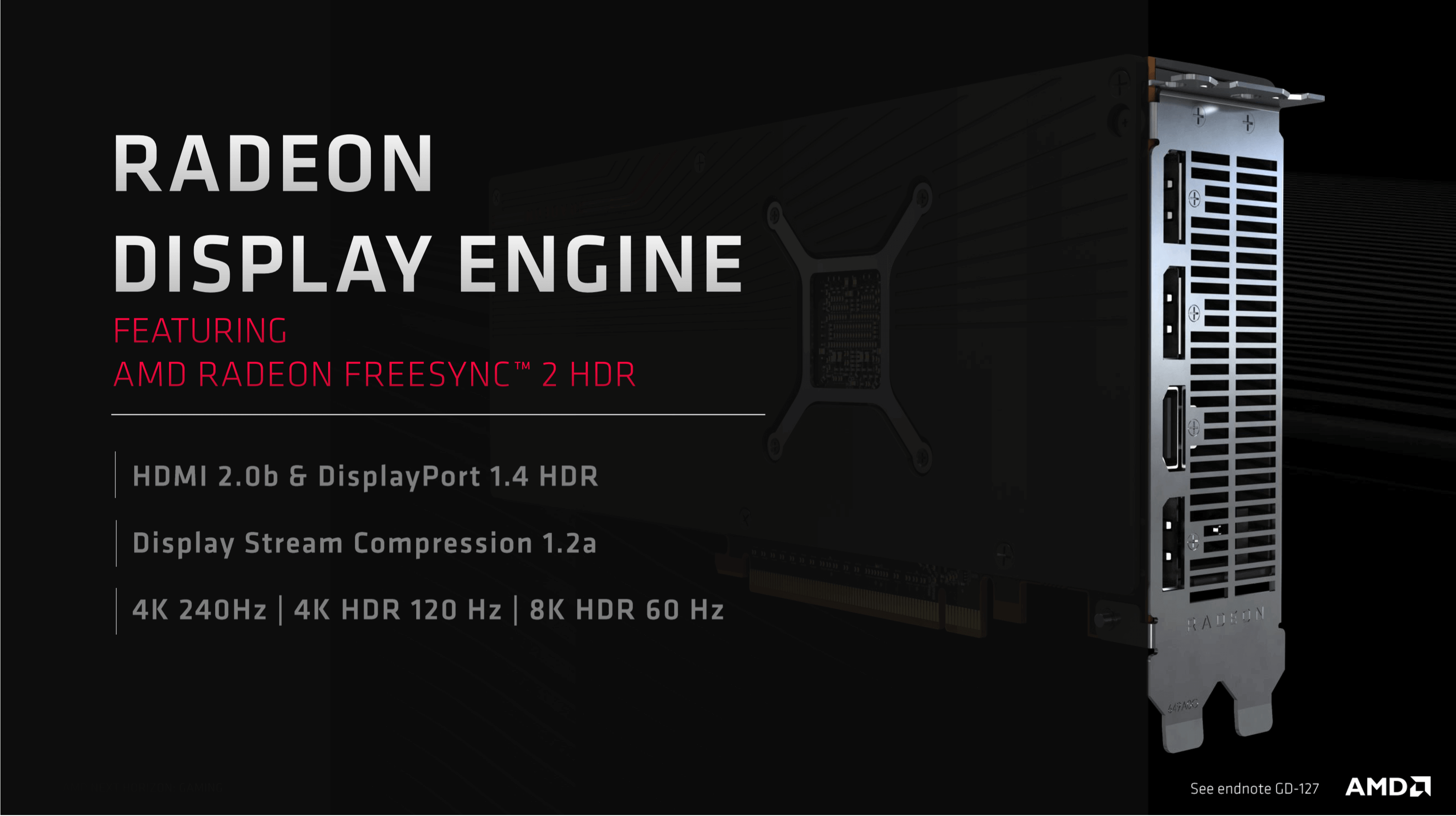
As you'd expect from a new 2019 GPU design, Navi's display engine offers very high resolutions, at high refresh rates, and offers HDR support. Display Stream Compression(DSC) is a fast lossy compression algorithm that allows for the likes of 4K+ resolutions at refresh rates more than 60 Hz to be transmitted over one DisplayPort 1.4 connection; fortunately the image quality degradation is very small, almost to the point that you'd consider DSC virtually lossless.
Turing also supports DisplayPort with DSC connections, although the supported high resolution and refresh rate combination is marginally better than in Navi: 4K HDR is at 144 Hz – but the rest is the same.
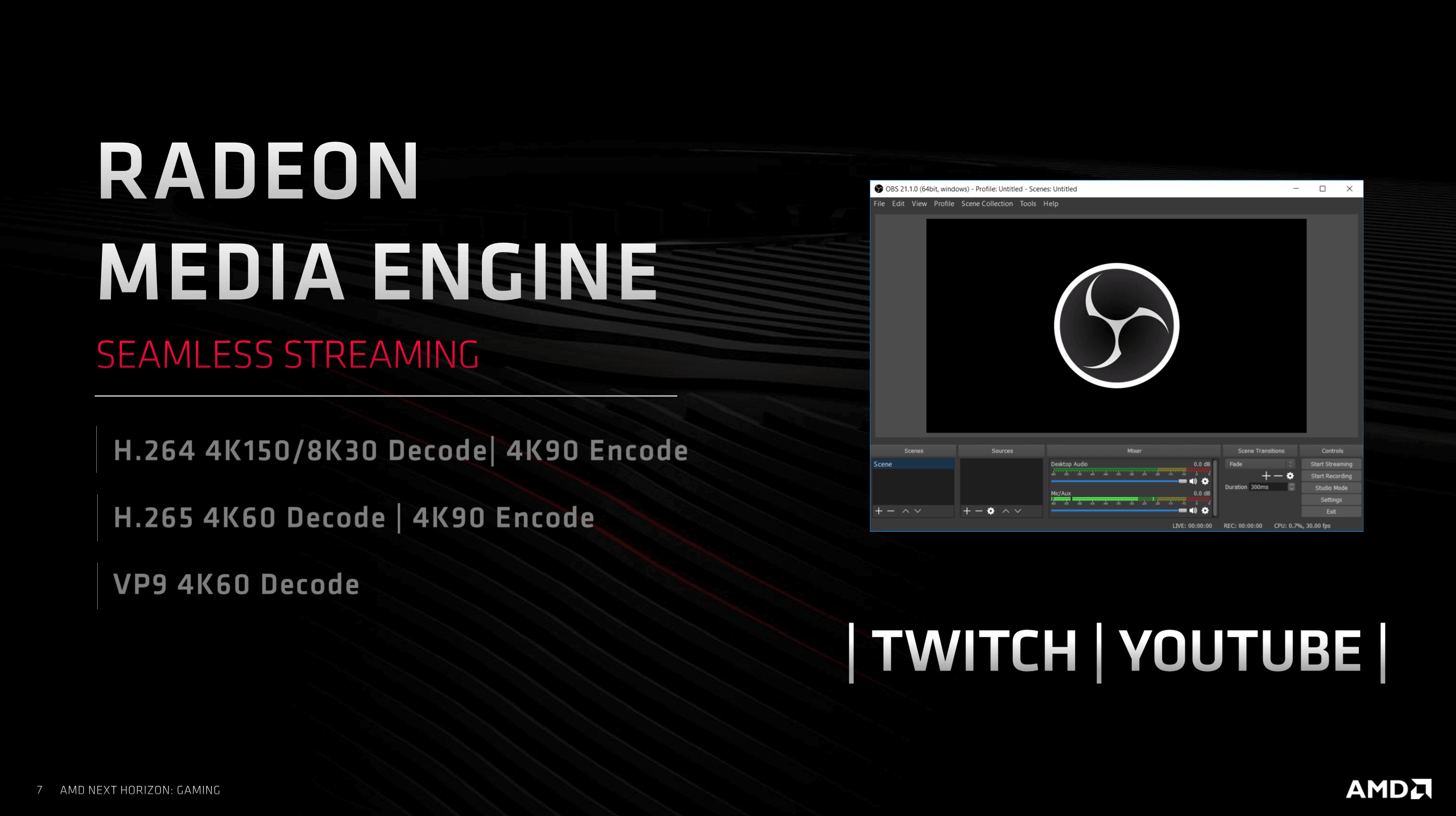
Navi's media engine is just as modern as its display engine, offering support for Advanced Video Coding (H.264) and High Efficiency Video Coding (H.265), again at high resolutions and high bitrates.
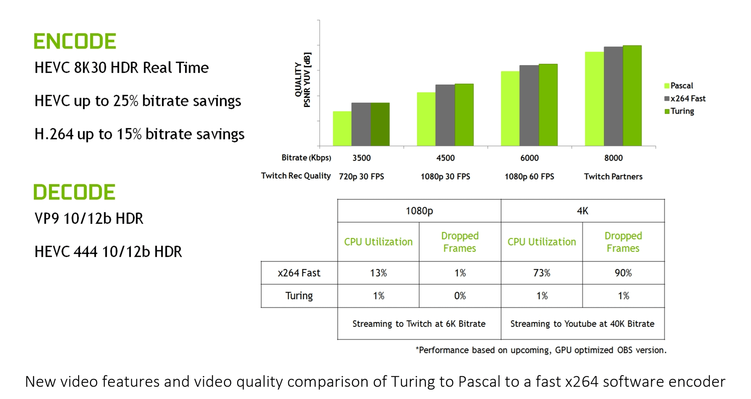
Turing's video engine is roughly the same as Navi's but the 8K30 HDR encoding support may tip the balance in favor of Turing for some people.
There are other aspects to compare (Navi's PCI Express 4.0 interface or Turing's NV Link, for example) but they're really just very minor parts of the overall architecture, no matter how much they get dressed up and marketed. This is simply because, for the vast majority of potential users, these unique features aren't going to matter.
Comparing Like-for-Like
This article is an observation of architectural design, features and functionality, but having a direct performance comparison would be a good way to round up such an analysis. However, matching the Navi chip in a Radeon RX 5700 XT against the Turing TU102 processor in a GeForce RTX 2080 Ti, for example, would be distinctly unfair, given that the latter has almost twice the number of unified shader units as the former. However, there is a version of the Turing chip that can be used for a comparison and that's the one in the GeForce RTX 2070 Super.
| ? | Radeon RX 5700 XT | GeForce RTX 2070 Super |
| GPU | Architecture | Navi 10 | RDNA | TU104 | Turing |
| Process | 7 nm TSMC | 12 nm TSMC |
| Die area (mm2) | 251 | 545 |
| Transistors (billions) | 10.3 | 13.6 |
| Block profile | 2 SE | 4 ACE | 40 CU | 5 GPC | 20 TPC | 40 SM |
| Unified shader cores | 2560 SP | 2560 CUDA |
| TMUs | 160 | 160 |
| ROPs | 64 | 64 |
| Base clock | 1605 MHz | 1605 MHz |
| Game clock | 1755 MHz | N/A |
| Boost clock | 1905 MHz | 1770 MHz |
| Memory | 8GB 256-bit GDDR6 | 8GB 256-bit GDDR6 |
| Memory bandwidth | 448 GBps | 448 GBps |
| Thermal Design Power (TDP) | 225 W | 215 W |
It's worth noting that the RTX 2070 Super is not a 'full' TU104 chip (one of the GPCs is disabled), so not all of those 13.6 transistors are active, which means the chips are roughly the same in terms of transistor count. At face value, the two GPUs seem very similar, especially if you just consider number of shader units, TMUs, ROPs, and the main memory systems.
In the Nvidia processor, one SM can handle 32 concurrent warps and with each warp consisting of 32 threads, a fully loaded GeForce RTX 2070 Super can work on 40,960 threads across the whole chip; for Navi, one CU can take up to 16 waves per SIMD32 ALU, with each wave being 32 threads. So the Radeon RX 5700 XT can also be packed with up to 40,960 threads. This would seem to make them exactly even here, but given how differently the CU/SMs are arranged, and Nvidia's advantage with concurrent INT and FP processing, the end result will depend heavily on the code being run.
This will have an impact on how various games performance because one 3D engine's code will favor one structure better than the other, depending on what types of instructions are routinely sent to the GPU. This was evident when we tested the two graphics cards:
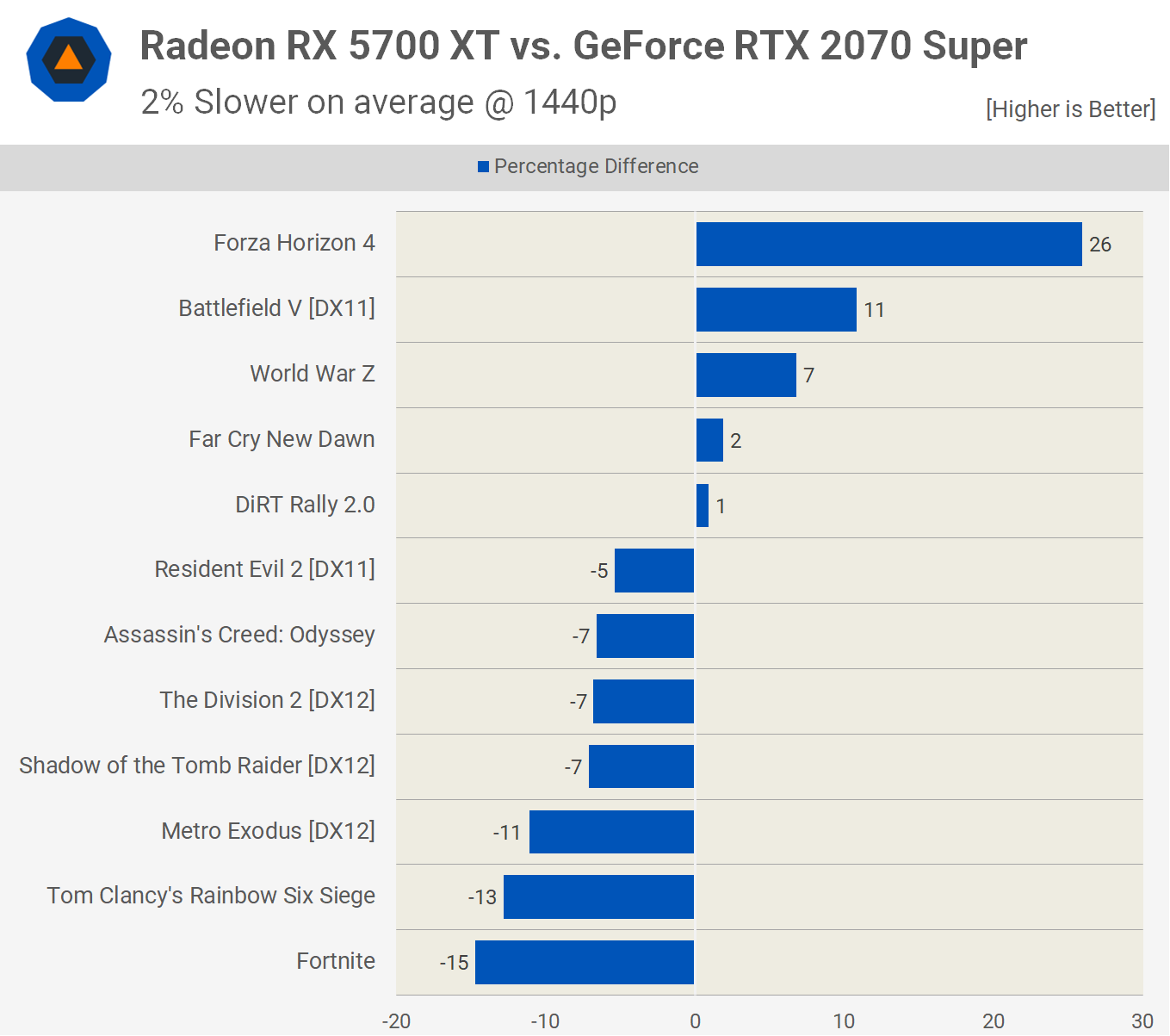
All of the games used in the test were programmed for AMD's GCN architecture, whether directly for Radeon equipped PCs or through the GCN GPUs found in the likes of the PlayStation 4 or Xbox One. It's possible that some of the more recently released ones could have prepped for RDNA's changes, but the differences seen in the benchmark results are more likely due to the rendering engines and the way the instructions and data are being handled.
So what does this all mean? Is one architecture really better than the other? Turing certainly offers more capability than Navi thanks to its Tensor and RT Cores, but the latter certainly competes in terms of 3D rendering performance. The differences seen in a 12 game sample just aren't conclusive enough to make any definitive judgment.
And that is good news for us.
Final Words
AMD's Navi plans were announced back in 2016, and although they didn't say very much back then, they were aiming for a 2018 launch. When that date came and went, the roadmap changed to 2019, but it was clear that Navi would be manufactured on a 7nm process node and the design would focus on improving performance.
That has certainly been the case and as we've seen in this article, AMD made architectural changes to allow it to compete alongside equivalent offerings from Nvidia. The new design benefits more than just PC users, as we know that Sony and Microsoft are going to use a variant of the chip in the forthcoming PlayStation 5 and next Xbox.
If you go back towards the start of this article and look again at the structural design of the Shader Engines, as well as the overall die size and transistor count, there is clearly scope for a 'big Navi' chip to go in a top-end graphics card; AMD have pretty much confirmed that this is part of their current plans, as well as aiming for a refinement of the architecture and fabrication process within the next two years.
But what about Nvidia, what are their plans for Turing and its successor? Surprisingly, very little has been confirmed by the company. Back in 2014, Nvidia updated their GPU roadmap to schedule the Pascal architecture for a 2016 launch (and met that target). In 2017, they announced the Tesla V100, using their Volta architecture, and it was this design that spawned Turing in 2018.
Since then, things have been rather quiet, and we've had to rely on rumors and news snippets, which are all generally saying the same thing: Nvidia's next architecture will be called Ampere, it will be fabricated by Samsung using their 7nm process node, and it's planned for 2020. Other than that, there's nothing else to go on. It's highly unlikely that the new chip will break tradition with the focus on scalar execution units, nor is it likely to drop aspects such as the Tensor Cores, as this would cause significant backwards compatibility issues.
We can make some reasoned guesses about what the next Nvidia GPU will be like, though. The company has invested a notable amount of time and money into ray tracing, and the support for it in games is only going to increase; so we can expect to see an improvement with the RT cores, either in terms of their capability or number per SM. If we assume that the rumor about using a 7 nm process node is true, then Nvidia will probably aim for a power reduction rather than outright clock speed increase, so that they can increase the number of GPCs. It's also possible that 7 nm is skipped, and Nvidia heads straight for 5 nm to gain an edge over AMD.
And it looks like AMD and Nvidia will be facing new competition in the discrete graphics card market from Intel, as we know they're planning to re-enter this sector, after a 20 year hiatus. Whether this new product (currently named Xe) will able to compete at the same level as Navi and Turing remains to be seen.
Meanwhile Intel has stayed alive in the GPU market throughout those 2 decades by making integrated graphics for their CPUs. Intel's latest GPU, the Gen 11, is more like AMD's architecture than Nvidia's as it uses vector ALUs that can process FP32 and INT32 data, but we don't know if the new graphics cards will be a direct evolution of this design.
What is certain is that the next few years are going to be very interesting, as long as the three giants of silicon structures continue to battle for our wallets. New GPU designs and architectures are going to push transistor counts, cache sizes, and shader capabilities; Navi and RDNA are the newest of them all, and have shown that every step forward, however small, can make a huge difference.
Shopping Shortcuts:
- GeForce RTX 2070 Super on Amazon
- GeForce RTX 2080 Super on Amazon
- GeForce RTX 2080 Ti on Amazon
- Radeon RX 5700 XT on Amazon
- Radeon RX 5700 on Amazon
- GeForce RTX 2060 Super on Amazon
- GeForce GTX 1660 Super on Amazon
This article was originally published in August 7, 2019. We've slightly revised it and bumped it as part of our #ThrowbackThursday initiative.